Project / Finished product
CTU SSTC
A tabletop SSTC for Czech Technical University. It has to live in an 80×30×30 cm shelf in PlasmaLab, with almost no air moving past it.
- Power electronics
- High voltage
- Status
- Finished product
- Bridge
- IRFP460
- Frequency
- 481 kHz
- Secondary
- 900 turns
- CW power
- 1 kW
At a glance
A shelf in PlasmaLab
After DRSSTC I, Czech Technical University in Prague asked for a very small tabletop solid-state Tesla coil. The only real constraints were the shelf, 80×30×30 cm, and the fact that almost no air circulates in it. The coil is on display in PlasmaLab at the Faculty of Nuclear Sciences and Physical Engineering.
It was the most frustrating coil I have built. Small means a high frequency, and a high frequency is awkward to drive. I settled on a half-bridge fed from a gate-drive transformer, and a UD2.7, because I already had one. It sounded simple. It was fail after fail. Months of it, at 660 kHz, before I gave up on that secondary and wound a new one with thinner wire and a larger topload.
The gates would not follow
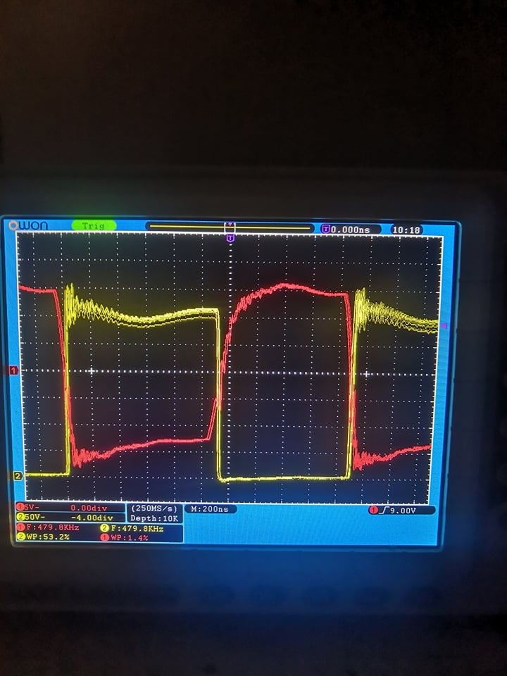
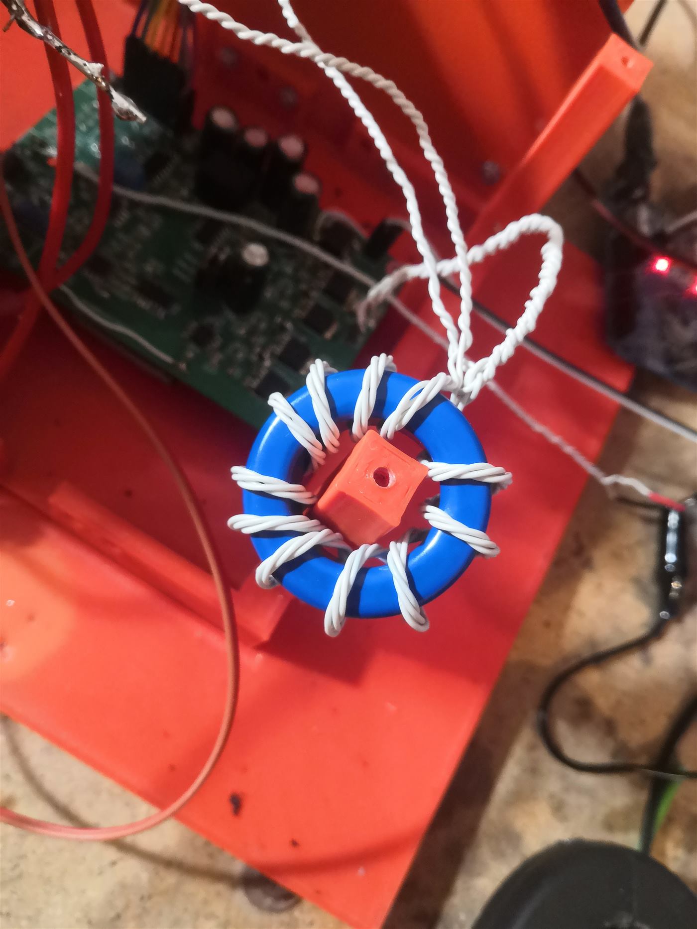
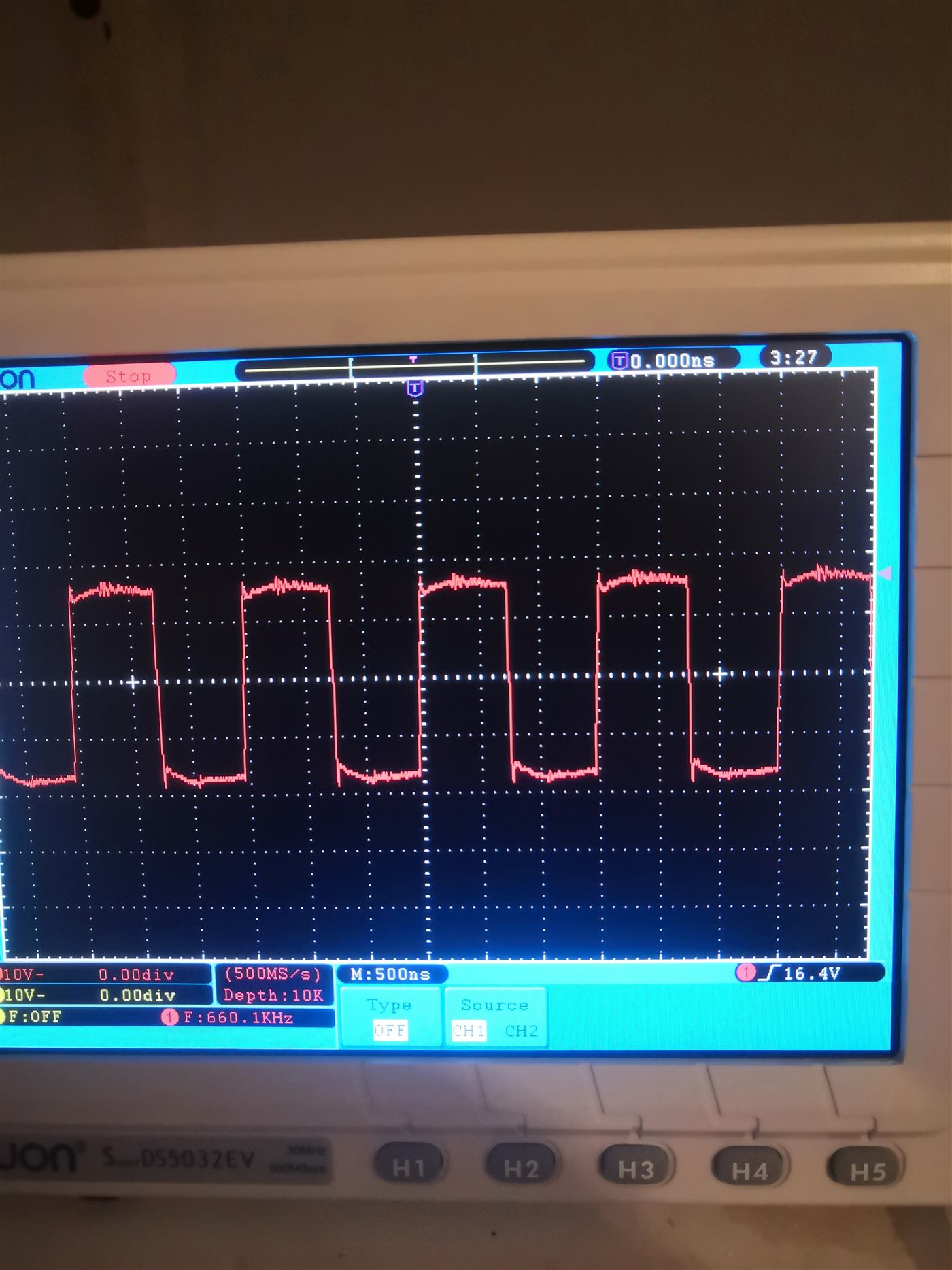
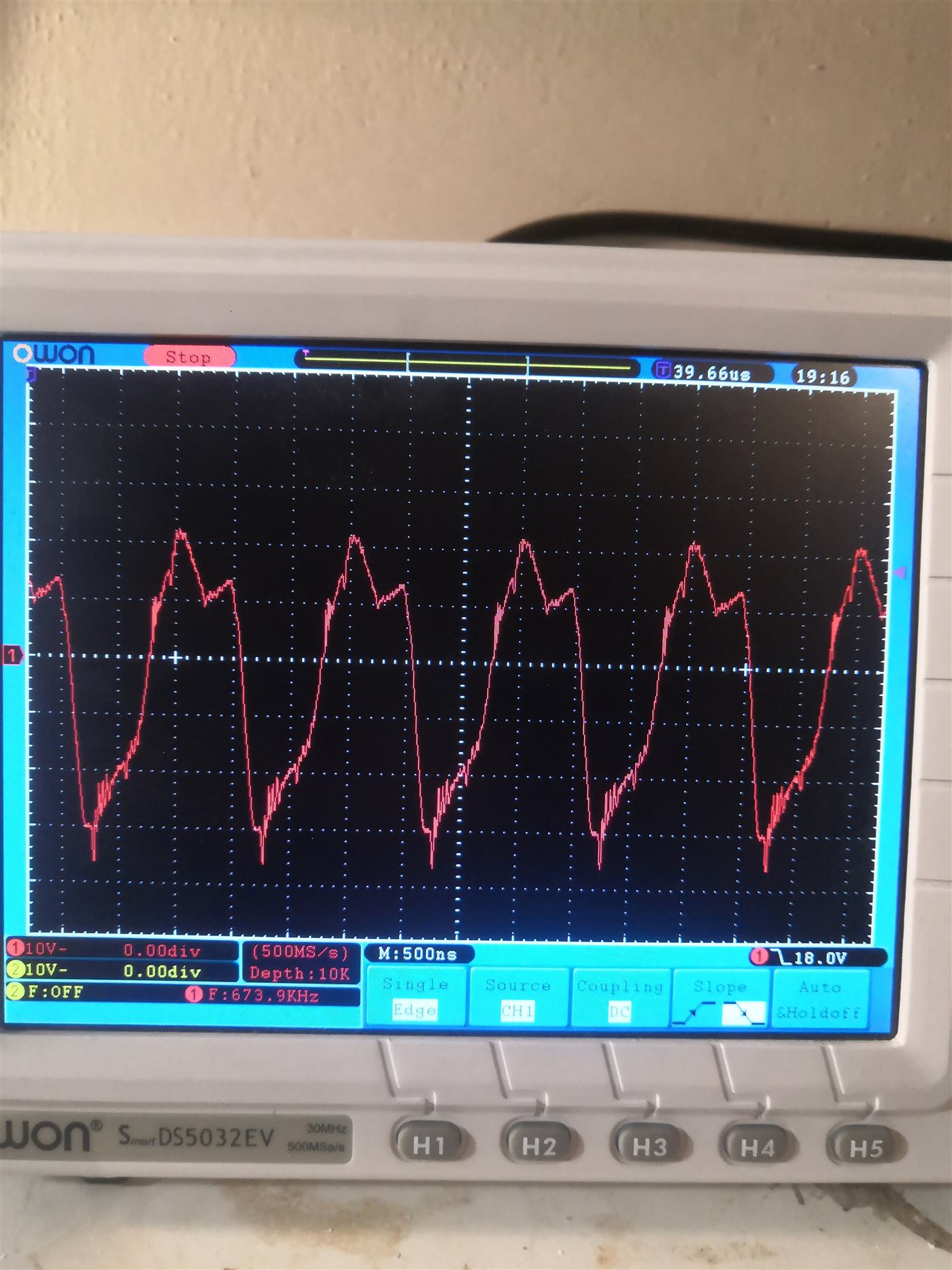
The real problem was the gates. I could not drive them properly at that frequency. I tried at least four gate-drive transformers, different sizes and different cores. All of them were poor at best.
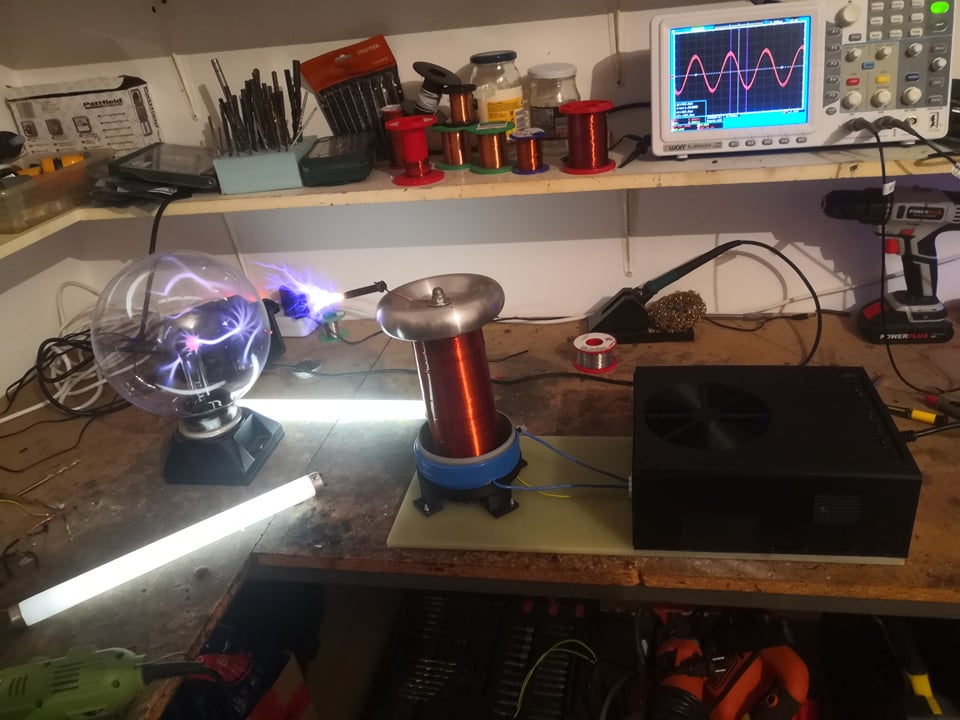
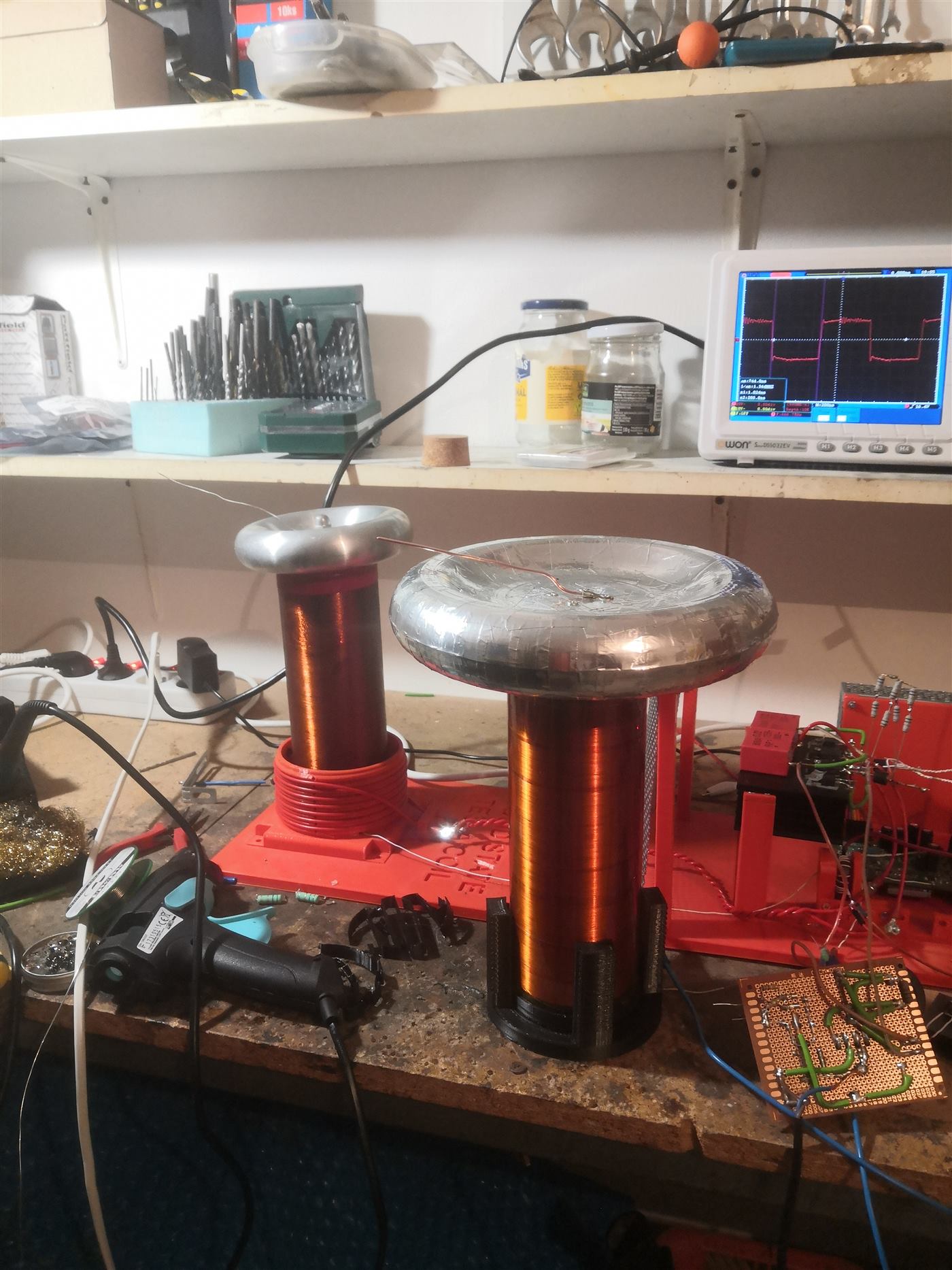
The primary side of the transformer looked fine. The secondary, the side the MOSFETs actually see, was unusable. A new secondary and a new topload brought the resonance down to about 400 kHz. The old 660 kHz coil is the one sitting behind it.
A driver from scratch
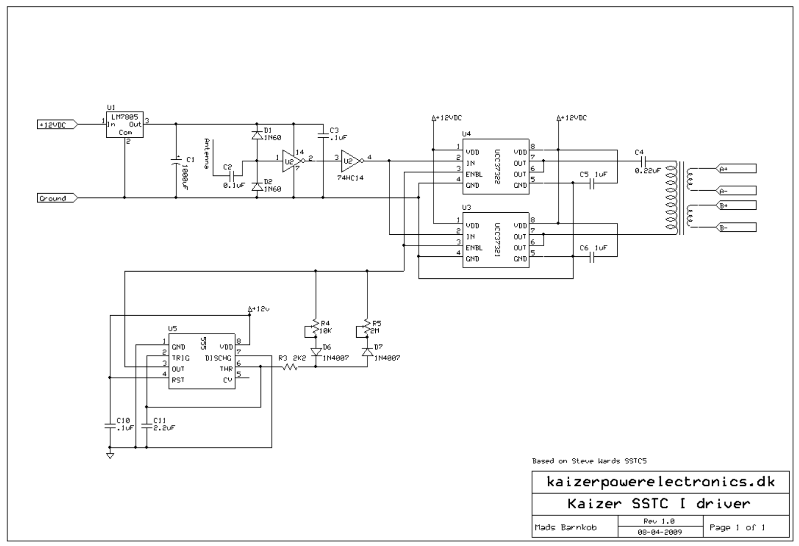
With the new secondary the resonance landed at 391 kHz. The gates still looked awful. Five core materials later I had a small improvement and one conclusion: the UD2.7 was not delivering enough current into the primary of the gate-drive transformer. I built a driver from scratch, along the lines of a classic SSTC driver. Antenna feedback, Schmitt inverters, and a pair of inverting and non-inverting FET drivers. The starting point was a schematic from Kaizer Power Electronics.
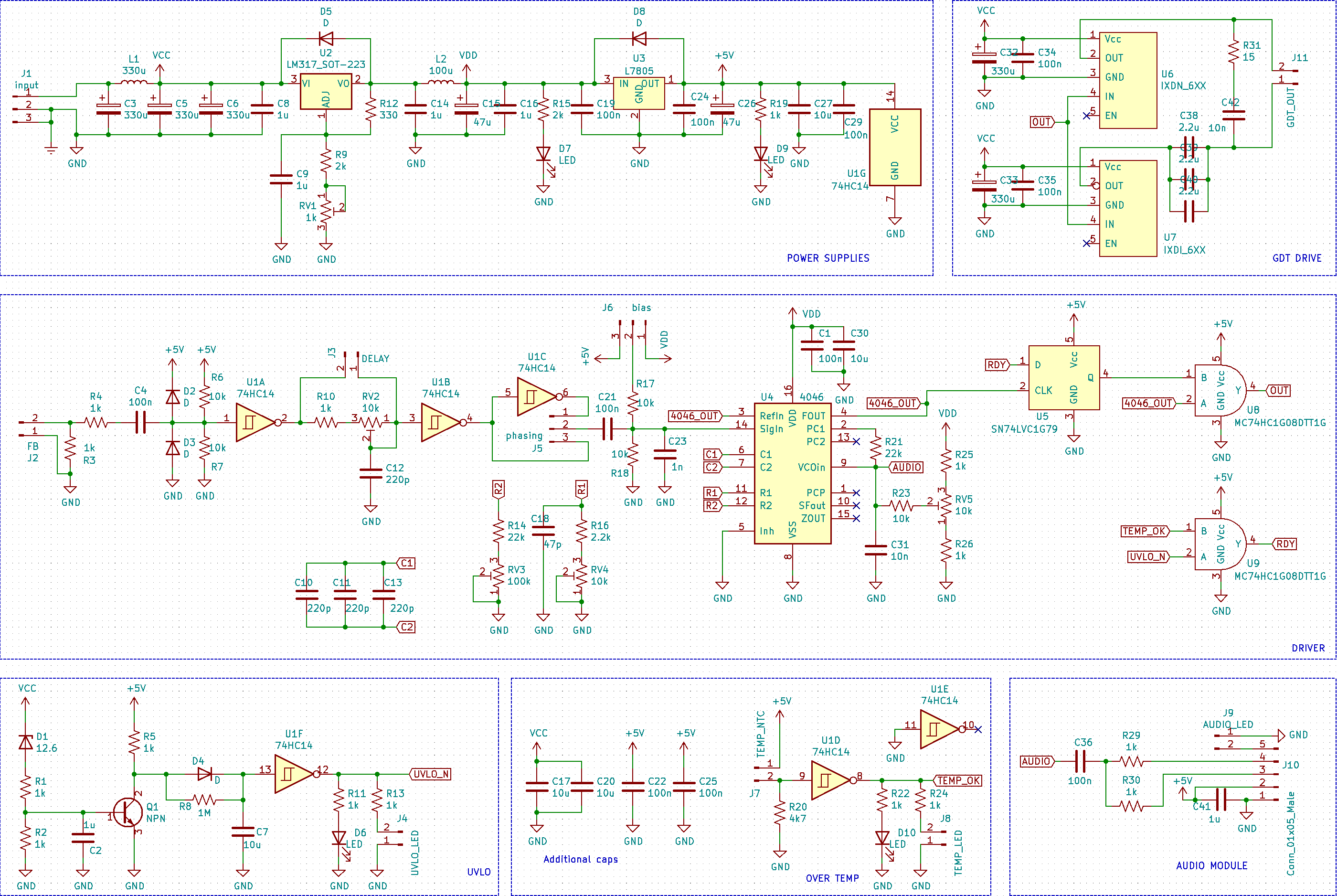
The antenna picks up the secondary. C2 blocks any DC that would pull the duty cycle off centre. D1 and D2 clamp the Schmitt inverters. The inverters turn the sine into a square, and that square goes to the FET drivers. C4 blocks DC again. The UCC37321 and UCC37322 have an enable pin, so the bridge can be interrupted to limit the power, or to play audio.
The gates finally looked promising, and then the new problems showed up. Even with C2 in circuit the duty cycle was not 50%. It was closer to 60:40. Worse, the feedback was noisy and sometimes the coil never started. The antenna was fussy. It had to sit in one exact place or the feedback would not catch.
Off the antenna
I dropped the antenna and used a feedback transformer. That fixed part of it. The transformer still listened to everything near the coil. Sometimes it locked onto 50 Hz from the mains before the secondary had started, and that is an easy way to kill the transistors.
So the feedback itself had to change.
A phase-locked driver
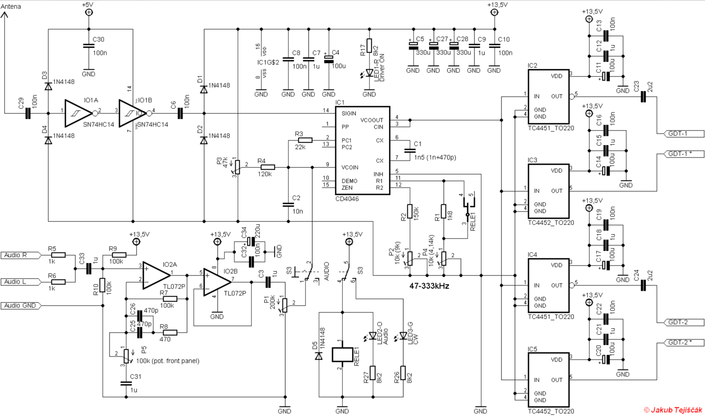
A phase-locked loop makes its own output, and the frequency of that output can be pulled. Three pieces: a voltage-controlled oscillator, a phase detector, and a low-pass filter. The oscillator goes into the phase detector, which compares it with the input and produces a square wave whose duty cycle is the phase error. The filter averages that square wave into a DC voltage, and the DC voltage steers the oscillator until the two phases match. It keeps oscillating with nothing on the input. Feed it a signal and it follows.
For an SSTC the oscillator is set as close as possible to the secondary resonance. Feedback from the secondary goes to the input of the loop. The coil starts at a sensible frequency, then the drive follows as the arc and the room move the resonance around. I was not inventing the circuit. The one I built from is on vn-experimenty, this time around a CD4046.
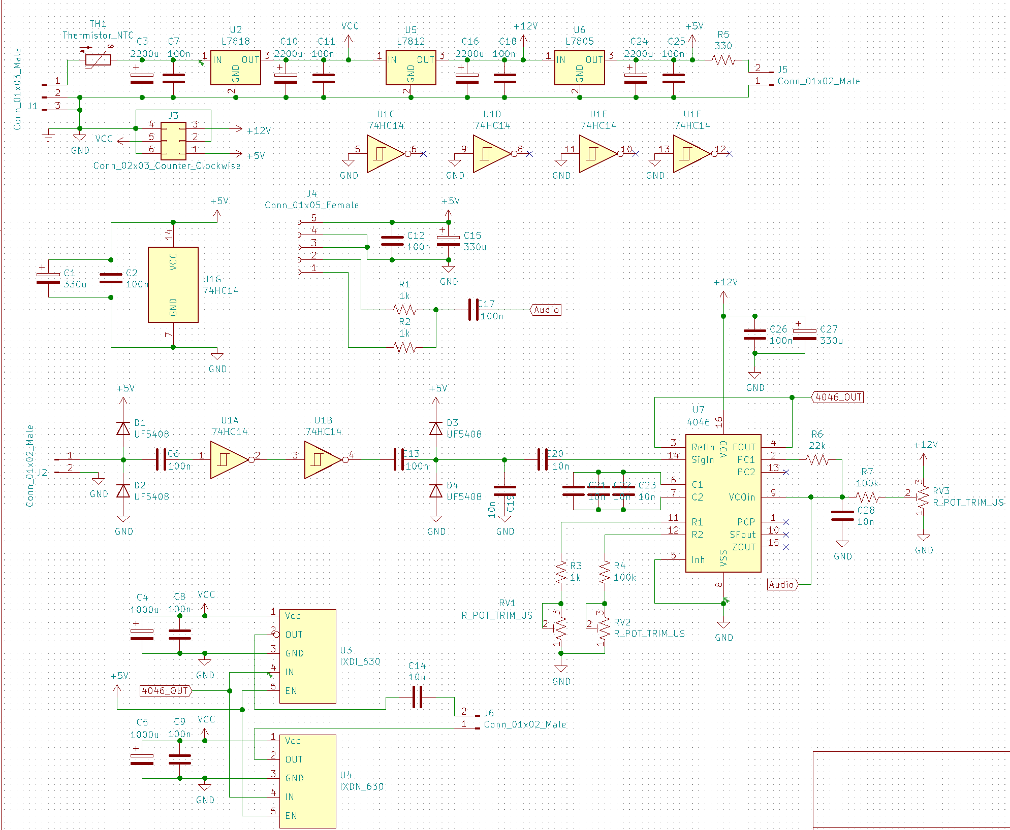
Feedback is a current transformer again, with clamp diodes and 74HC14 Schmitt inverters. C6 strips DC before the 4046, and the 4046 input is clamped too. R3 and C2 are the loop filter. Pin 9, VCOIN, is the voltage that sets the frequency. The loop only works inside a window, so the potentiometer puts the free-running frequency in the middle of that window. R1 and C1 set the frequency, R1 and R2 set how far it can swing, and the 4046 output goes to FET drivers on the primary of the gate-drive transformer. A further 10 nF after C6 helps: the CD4046 does not like sharp edges. The TC4451 and TC4452 have no enable pin, so an AND gate mixes a simple interrupter with the 74HC14.
Ten centimetres, then a melted toroid
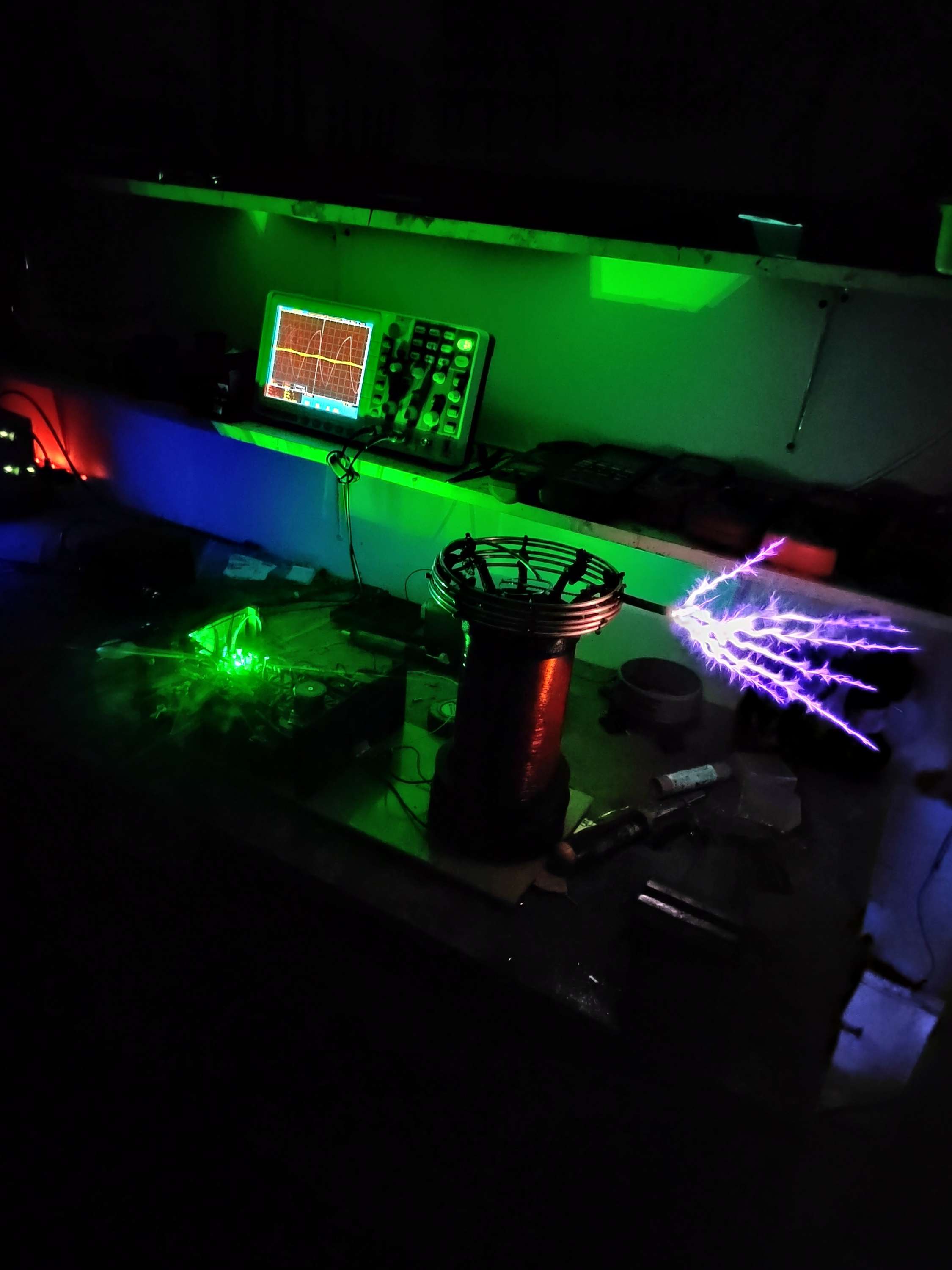
At about 120 V AC and 50% duty I finally had sparks, about 10 cm. Turn the duty past 80% and the topload got hot enough to melt the plastic it was printed from. I make toploads as a PLA toroid wrapped in aluminium tape. The glue on that tape does not conduct, so the layers are not really connected to each other. It is enough capacitance. It is not enough conductor once the duty cycle is high and the current has somewhere to go. The previous secondary had a solid metal topload. Smaller, but metal.
With that topload the resonance moved up to 481 kHz. I expected the gate-drive transformer to fall apart again. After C1 in the PLL was set for the new frequency, the gate waveforms looked almost the same as they had at 390 kHz. I took a few turns off the primary and raised the coupling for more power.
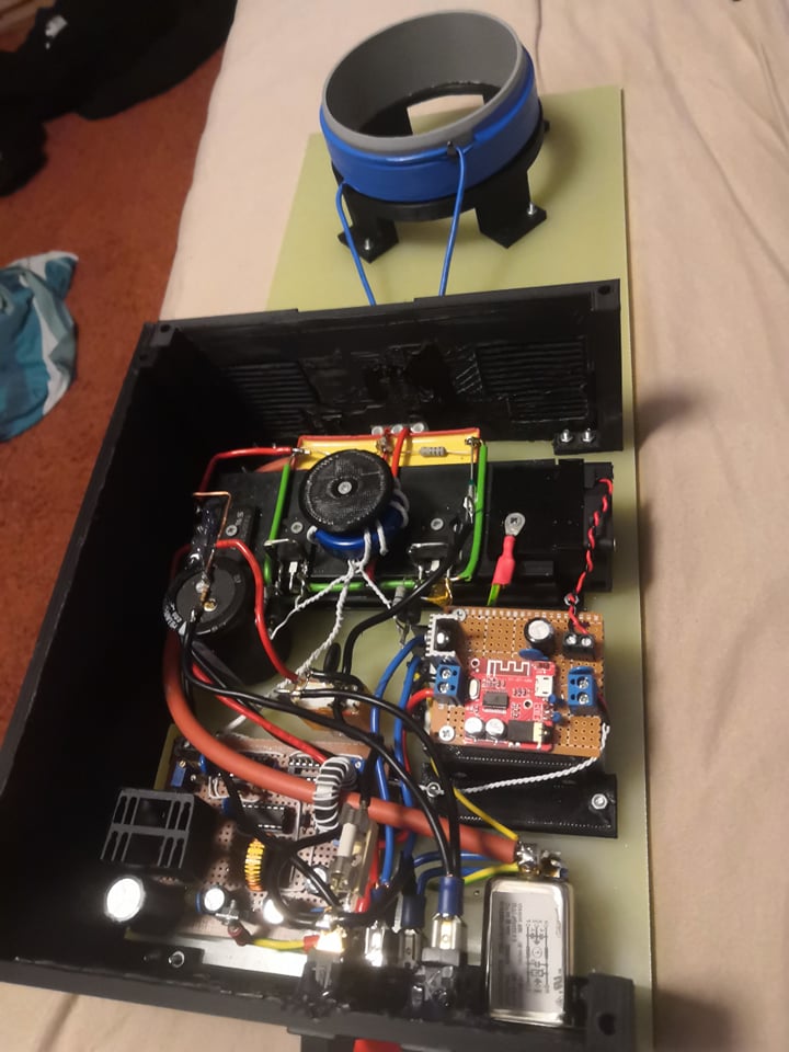
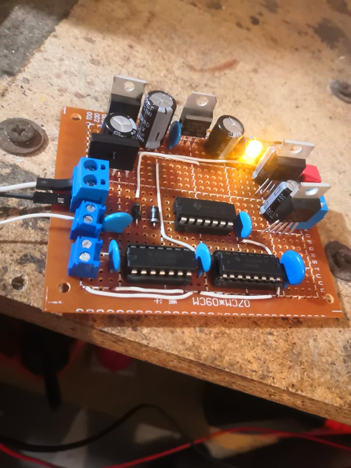
The whole thing was built while it was running, so I never drew that exact board. It is close to the schematic above. School left little time for notes, and these are most of the pictures I have. A full-bridge PLL SSTC, documented properly, was the plan.
Three ways to feed it
I had wanted an interrupter to limit the power. What I actually built is simpler. Three modes: a single diode, so 50 Hz with no smoothing; a full bridge, so 100 Hz with no smoothing; and a full bridge plus a 680 µF capacitor, which is CW. Roughly 500 W, 750 W, and 1 kW.
At 50 Hz it will run indefinitely without overheating. I never really tested 100 Hz, but it should be fine. CW is different. The primary is hot within minutes and at 90 °C after about ten. The primary is the limit. The secondary stays cooler, and the transistors are only warm — until the lid is on. In the closed box they reach about 60 °C after ten minutes of CW, even with two fans on the heatsink.
Audio on the VCO
A PLL is easy to modulate. Couple audio straight onto the VCO and the drive frequency moves. I used a small Bluetooth board that takes audio from a phone and feeds the oscillator. The level is about what a headphone jack produces, roughly 1 V peak to peak, and that is enough to shift the driver by ±6 kHz. Loud enough, and clean, which is the part that mattered.
The Bluetooth module also brings galvanic isolation with it. That is most of why it belongs on this coil.
As it left the bench
Half-bridge of IRFP460s, CD4046BE, three power modes, and a resonance just under 500 kHz. These are the notes I would hand to the next person who opens the case.
Specification
- Driver: CD4046BE PLL, half-bridge of IRFP460
- Modes: 50 Hz, 100 Hz, and CW, with Bluetooth audio
- Power: about 500 W, 750 W, and 1 kW
- Frequency: 481 kHz, 473 kHz with an arc
- Secondary: 900 turns of 0.2 mm double enamel
- CW bus capacitor: 680 µF. Topload about 3×11 cm
- Breakout: graphite rod from a 9 V battery
What stuck
- A PLL is the most reliable way I have found to drive an SSTC.
- IRFP460s are usually robust enough. A newer FET is not automatically a better one.
- Coupling between primary and secondary is what sets the power draw.
- Gate-driver ICs belong on a heatsink. DIP packages overheat.
- Tie the driver ground to mains earth and to the bottom of the secondary.
- Keep at least a few nanofarads in the PLL oscillator. Smaller, and it gets too sensitive.
- Interrupted sparks are longer than CW arcs.
- A small glitch in the logic can wreck the gate waveforms.
- Anything that fails should be easy to reach and easy to replace.
- Linear regulators hate inrush. An NTC in series with the supply.
- The breakout cannot be copper. In CW the plasma melts it immediately.
The next board
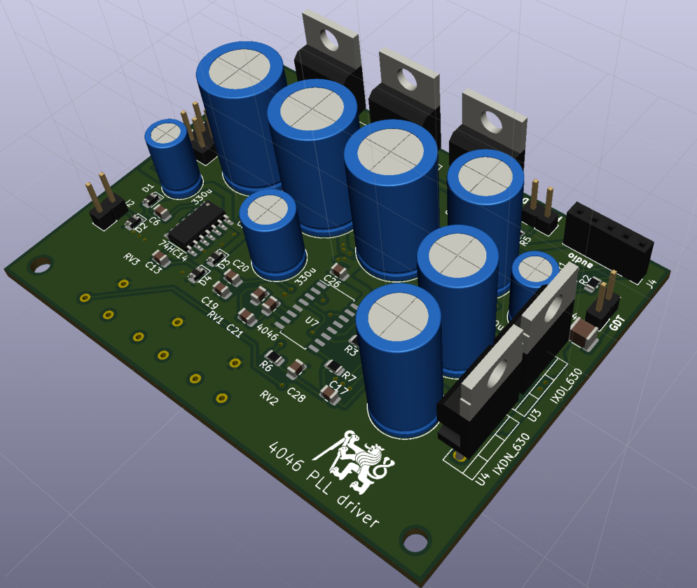
It was a struggle, and it was worth it. It is the reason I kept building PLL SSTCs. While I was writing the original notes I was already laying out a small SMD driver, 8×6 cm, with gate drivers that can actually be bolted to a heatsink.
The same coil also picked the topic of my bachelor thesis: a universal inverter driver on an STM32 or an FPGA. Any FET or IGBT, fixed frequency or PLL, from about 1 kHz to 1 MHz, with overcurrent, overtemperature, undervoltage, and short-circuit detection, and galvanic isolation that does not depend on a gate-drive transformer. In principle the same board would drive a PC supply, a bench supply, an induction heater, or a DRSSTC.
Brought back cooked
In January 2024 the coil came back damaged. The report I was given did not really add up. Someone preferred not to own it. From the hardware, it had simply been left running. The primary insulation had melted into the PVC pipe it was wound on.
Both switches were dead. A new pair should have been the whole repair. After they were in, the driver behaved strangely. The PLL would not lock, and after a few changes to the drive circuit one of the gate-driver ICs went short. I still do not know what killed that IC. The driver was on a protoboard by then and had turned into a mess, so it needed a new board anyway.
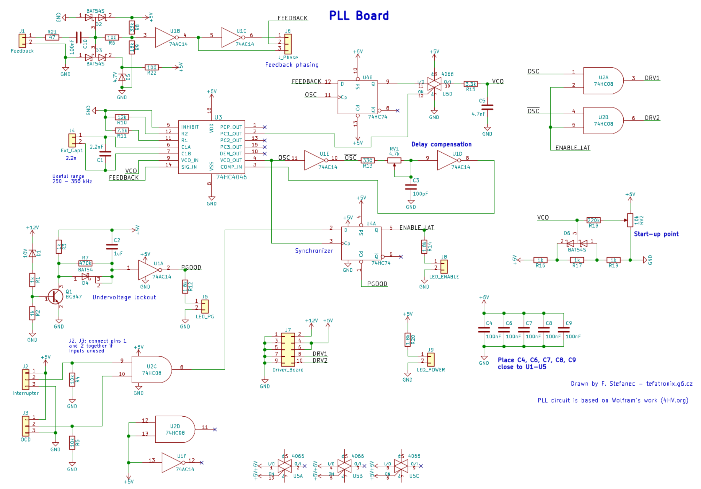
The tidy PCB from the section above ended up in SSTC II. For this coil I wanted to try a phase lag in the feedback. I had not realised an SSTC can run at zero-current switching, so the earlier ones were inefficient. ZCS needs a delay in the feedback path. One version of that delay sits between pins 4 and 3 of the CD4046. The drawing I started from is by Tefatronix.
Finding the phase
I put the same idea directly in the feedback, between the current transformer and pin 14 of the CD4046. A D flip-flop and a few AND and OR gates watch undervoltage and overtemperature. The flip-flop only acts between cycles, so a trip does not turn a transistor off in the middle of a high-current pulse. If the coil is in ZCS, that avoids the spike you get from interrupting primary current.
Jumpers bypass the delay, and a second set tries bias voltages on the 4046. It locks properly only when the input is biased at half VDD. Tied to 5 V, or left open, it does not lock at all. The delay itself was a disappointment. On a signal generator the output phase moved. In the coil, with real feedback, the switching phase did not. The fix was on Jakub Tejisčák’s site, which is where I had taken the PLL idea from in the first place. His SSTC sets the phase with a potentiometer on pin 12, R2. The centre frequency, set by R1 and R2, moves the output phase. I did the same with R1. That worked.
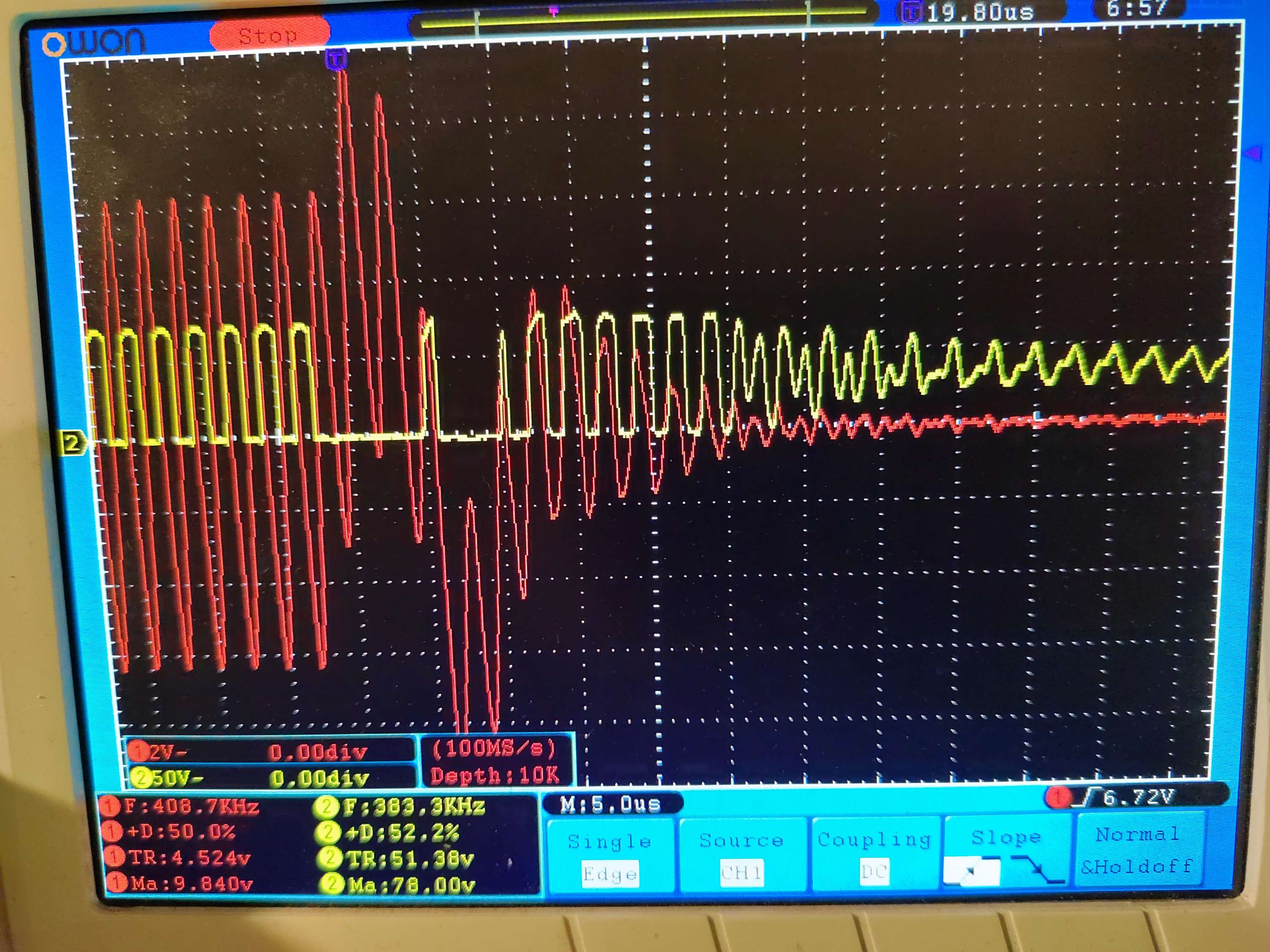
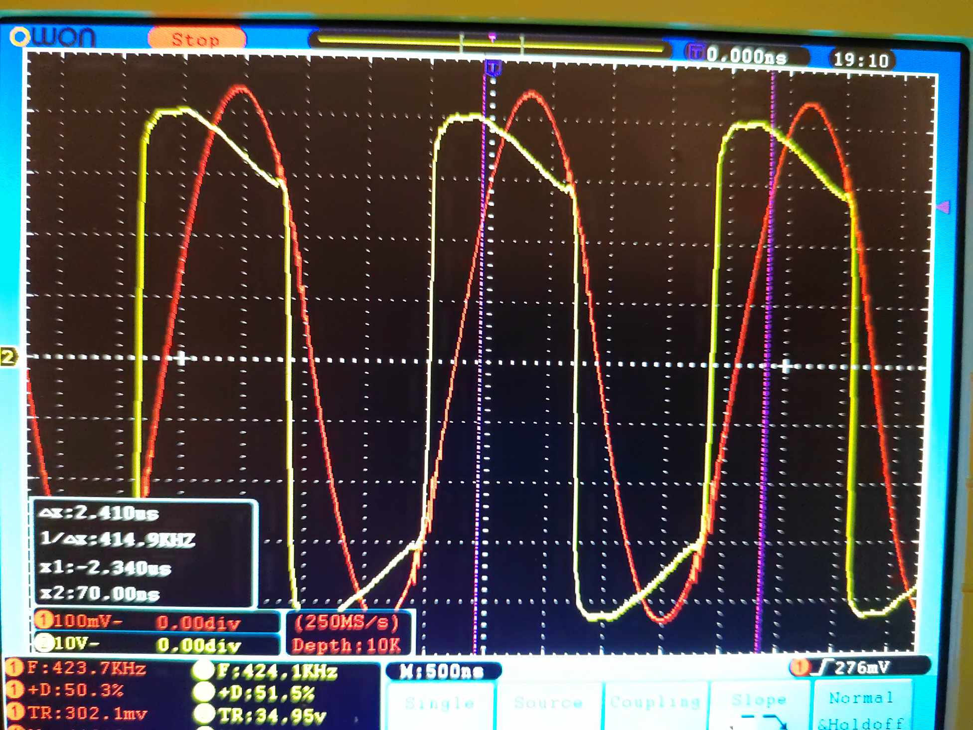
On the scope it can look as if the bridge voltage misses the current zero. The lag is the bridge waiting while the MOSFET output capacitance and the snubbers charge. Push the phase any closer to the zero and it gets less efficient and much noisier. This setting is clean. The capture is at 100 V on the DC bus, primary current 6 A rms. The old secondary was overheating, so it came off. The new one is about 800 turns of 0.3 mm on 10 cm PVC, 18 cm long.
A second primary
Once ZCS was tuned, the transistors stayed under the overtemperature trip. The primary was the part that got hot. I wound a second primary in parallel, the same wire, as a double coil. Resistance drops, so the copper should run cooler. Coupling rises too, because the winding now climbs further up the secondary. Input power went up 53%. The sparks grew with it, and so did the transistors. Overtemperature, about 60 °C, tripped after 1 minute 28 seconds of CW at 1150 W.
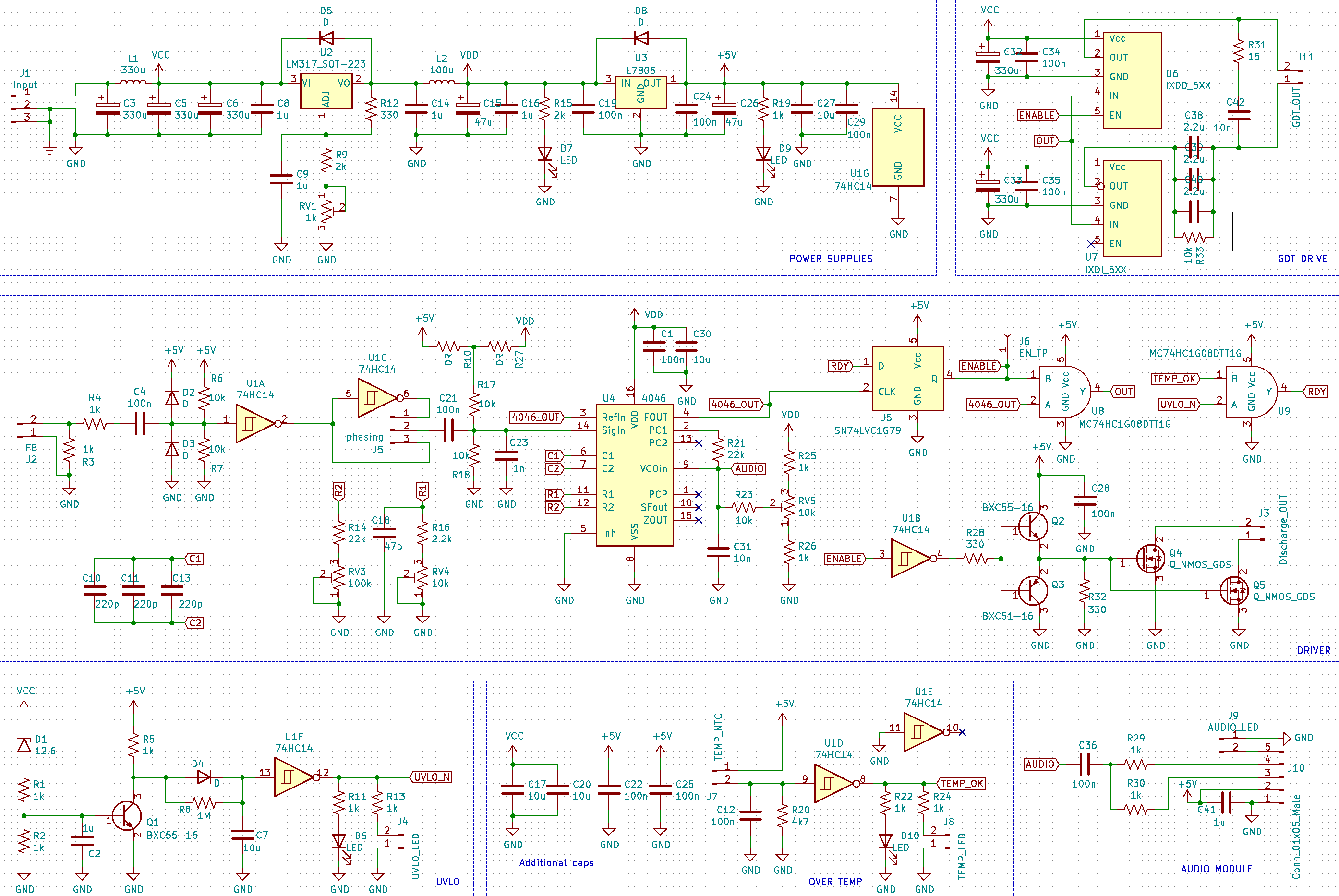
That is also when they died. The undervoltage and overtemperature lockouts had a bad hole. A trip forces a logic low into the gate drivers. One of those drivers inverts, so the two outputs become low and high, and the full bus sits across the primary. The DC blocking capacitors stop that from being a short. They also leave the gate-drive secondaries with nowhere to dump their charge, so one MOSFET stays on. The gate only bleeds down through the transformer winding, over several cycles. I had already seen a hint of it, triggering undervoltage by hand at low voltage. The primary current looks as if it is riding on a second sine. At about 80 V DC the transistors survived. At 325 V DC, LTspice put more than 14 kW of peak loss on one of them.
The next board shorts the leftover gate charge to ground through another winding on the gate-drive transformer. One driver changed from IXDN to IXDD, because the IXDN does not use its enable pin. R33 bleeds DC off the blocking capacitors so they sit at zero when enable goes high again. The unused phase-lag circuit came off. I was waiting on that PCB when I wrote the repair up. The 60 °C in 88 seconds was with the heatsink fan off, so with the fan the switches should be fine. 60 °C is not that hot. The trip could sit higher.